EE 103: Intro to VLSI Desig, EE103
Tufts University, Fall 2013
By Leiny Garcia and Nana Kwasi Kwakwa
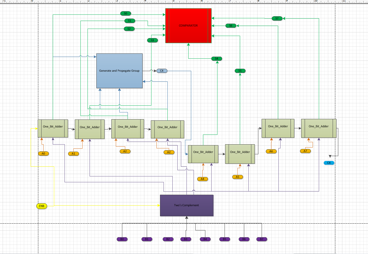
This project consists of an 8-bit Adder that was designed using Cadence Design System. The goals for this project were:

In the Adder and Subtractor design, an intuitive source of delay is the carry out that propogates through cascaded one bit adders. The consecutive one bit adder must wait for the previous adders to finish calculating. With this problem in mind, asymmetrical gates were used in the logic of the sum, carry out of one bit adder, and the fourth carry of a four cascaded one bit adder. The Asymetrical XOR was used for the Sum, because, due to the limited transistors available, the sum must go through two XOR's. These gates are the biggest source of delay since the logical effort of an XOR is 4ns. The second stage of XOR was replaced with an asymetrical XOR. In the case of the carry out of a one bit adder, the inputs go through two stages of NAND gates. Therefore, an asymmetrical NAND gate was placed in the second stage in providing Carry out. Finally, the CLA determines the value of carry out using logic that includes a group Generate and Propogate Output. The grouping logic is another source of delay. The NAND gates in the CLA logic were replaced with asymetrical NAND.
An Asymmetrical Logic Gate is used when a circuit has inputs that take a while to arrive to the transistor.This way, while the transistor is waiting for the second input, the early input can start charging most of the capacitors in the transistor, leaving the later input with lower capacitance to charge. As a result, the transistor quickly produces an output when the second input arrives. The logical effort of the late input is smaller than the early input in order for the transistor to output faster. In this gate, input A has a large logical effort of 2ns, compared to the logical effort of 1.5ns from input B.Therefore, input A is used for early inputs, and input B is used for later inputs. A Layout could not be made that would pass LVS and DRC, therefore a Post Simulation could not be made with this gate to compare the results. However, the spectre simulations shows worst case delay improvement when using this asymetrical gate in the Adder and Subtractor.The average logical effort of this gate is 1.75ns.
This XOR gate has sizes that provide a small logical effor for the later Input B, and a large of this gate has a smaller logical effort than that of A. The average general effort was calculated to be 2.52, because the average effort of the XOR gate is 1.8, but we wanted to account for the inverters that were added to the gate in order to increase the power. Without the inverters, the XOR gate rises slowly. The inverters should have a logical gate of 1, however, in cadence the sizes are not that of a unit inverter. The inverter size was comparted to the unit inverter, and a logical effort 1.4.
This Adder not only produces a Sum and Carry Out, but also generate and propogate values. These determine whether there will exist a carry out in the end of cascaded one bit adders. In this design, the one-bit adder is cascaded to create a four-bit adder.Generate is the carry that is produced from adding A and B. Propogate is the carry that is produced if a propogating carry would be added to A and B.
Inputs for the Post Layout Simulation were A, B, C with a period of 50ns and Delay of 10ns, 15ns, and 25ns.
This CLA determines the value of C4 using the generate and propogate outputs of the one bit adder. The G and P are grouped. This circuit originally consisted ofand and or gates, but bubble pushing was used to change the circuit to only NAND gates.
The first Post Layout link shows the inputs used to test the CLA, and the last link shows the out\ puts.
The first two Post Layout links show the inputs used to test the FBA with CLA, and the third link shows the out\ puts.
This circuit is used for subtraction. When subtracting bits, the two's complement of second set of bits are added to the first set. In order to get the Two's Complement, the bits must be toggled and then added with a 1 (decimal value). The XOR takes in the bits that need to be toggled, and also inputs an enable that determines whether the circuit needs to add (enable=0) or subtract(enable=1). The same enable is Cin of the circuit in order to add the one bit needed to obtain the two's complement of the inputs.There was an LVS problem with the layout, so a post layout simulation could not be performed.
The first two Post Layout links show the inputs used to test the One's Complement, and the last link shows the outputs.
The Behavioral Simulation shows the functionality for test inputs requested in previous labs, which were
01111111+00000001
100001111+01111111
10000000-00000001
01111111-10001111
The final Adder and Subtractor design was tested with the worst case, which is adding 11111111+11111111 because there is a carry in each case. The spectre simulations below show a small improvement in delay using the asymetrical gates. The output of the Adder/Subtractor with the Asymmetrical gates begins to change a few nanoseconds before the Adder/Subtractor without Asymmetrical gates.
A magnitude comparator is a combinational circuit that compares two numbers, say, A and B, to determine whether A>B, A
Comparator 4-bit
Each magnitude comparator has 3 outputs but only outputs an exclusive set bit to indicate the relationship between A and B.
A 9-bit magnitude comparator comprised of 3 4-bit magnitude comparators.
4-bit magnitude comparators were stacked in order to form a 9-bit magnitude comparator.The comparators were stand alone units and thus had to be linked together using combinational logic. A customized cell was designed and implemented to cascade multiple standalone magnitude comparators of varying sizes.
The 9-bit registers were built by stacking multiple D-latches.
A look at the evolution of the design of the Comparison Module.
The original concept design of the TS9BMC is shown above. The approach was abandoned because it required a complex clocking synchronization.
The second approach simplified the necessary clock input sequence. However, the implementation was still a challenge. This approach was also abandoned.
This final schematic showed promise of simpler clocking complexity but was not implemented due to a lack of time. This two-sum comparator would always compare the current sum to a previous sum stored in the 9-bit register.
Using asymetrical gates has little impact in speed. As one can see from the results, the gates are not a great method to produce high speed circuits. These gates can be used for small changes in speed. However, the asymetrical gates did produce a shorter delay. The average delay for each sum bit output was .3ns.
Area: 0.37 millimeters squared
Each individual module of the Two-Sum 9-Bit Magnitude Comparator (TS9BMC) was successfully simulated and laid out however, integration was unsuccessful. With added time, the full integration of the adder/subtractor with the TS9BMC. The greatest challenge in implementing the TS9BMC is the synchroonizing of the clocking sequence. The original design involved the use of a demultipexer which required a higher level of complexity in clocking.
Area: 0.16 - 0.29 millimeters squared. Area increased as implementation complexity increased.